- 您现在的位置:买卖IC网 > Sheet目录489 > NTHD5903T1G (ON Semiconductor)MOSFET PWR P-CH DUAL20V CHIPFET
�� �
�
�NTHD5903�
�SOLDERING� FOOTPRINT*�
�0� .45� 7�
�2� .03� 2�
�0.08�
�2.03� 2�
�0.08�
�0.018�
�0� .63� 5�
�0.025�
�0� .63� 5�
�0.025�
�1� .09� 2�
�0.043�
�0� .17� 8�
�0.007�
�0� .45� 7�
�0.018�
�0.66�
�0.026�
�0.711�
�0.028�
�0.66�
�0.026�
�0.25� 4�
�0.010�
�SCALE� 20:1�
�mm�
�inches�
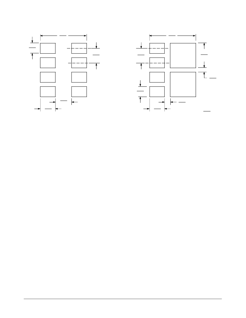
�Figure� 12.� Basic�
�Figure� 13.� Style� 2�
�*For� additional� information� on� our� Pb?Free� strategy� and� soldering�
�details,� please� download� the� ON� Semiconductor� Soldering� and�
�Mounting� Techniques� Reference� Manual,� SOLDERRM/D.�
�BASIC� PAD� PATTERNS�
�The� basic� pad� layout� with� dimensions� is� shown� in�
�Figure� 12.� This� is� sufficient� for� low� power� dissipation�
�MOSFET� applications,� but� power� semiconductor�
�performance� requires� a� greater� copper� pad� area,�
�particularly� for� the� drain� leads.�
�The� minimum� recommended� pad� pattern� shown� in�
�Figure� 13� improves� the� thermal� area� of� the� drain�
�confines� of� the� basic� footprint.� The� drain� copper� area� is�
�0.0019� sq.� in.� (or� 1.22� sq.� mm).� This� will� assist� the� power�
�dissipation� path� away� from� the� device� (through� the� copper�
�leadframe)� and� into� the� board� and� exterior� chassis� (if�
�applicable)� for� the� single� device.� The� addition� of� a� further�
�copper� area� and/or� the� addition� of� vias� to� other� board� layers�
�will� enhance� the� performance� still� further.�
�connections� (pins� 5,� 6,� 7,� 8)� while� remaining� within� the�
�http://onsemi.com�
�5�
�发布紧急采购,3分钟左右您将得到回复。
相关PDF资料
NTHD5904NT1G
MOSFET N-CHAN 3.3A 20V CHIPFET
NTHS2101PT1
MOSFET P-CH 8V 5.4A CHIPFET
NTHS4101PT1G
MOSFET P-CH 20V 4.8A CHIPFET
NTHS4166NT1G
MOSFET N-CH 30V 4.9A CHIPFET
NTHS4501NT1G
MOSFET N-CH 30V 4.9A CHIPFET
NTHS5404T1G
MOSFET N-CH 20V 5.2A CHIPFET
NTHS5441T1G
MOSFET PWR P-CH 3.9A 20V CHIPFET
NTHS5443T1
MOSFET P-CH 20V 3.6A CHIPFET
相关代理商/技术参数
NTHD5904N
制造商:ONSEMI 制造商全称:ON Semiconductor 功能描述:Power MOSFET 20 V, 4.5 A, Dual N−Channel, ChipFET
NTHD5904N_05
制造商:ONSEMI 制造商全称:ON Semiconductor 功能描述:Power MOSFET 20 V, 4.5 A, Dual N−Channel, ChipFET
NTHD5904NT1
功能描述:MOSFET 20V 4.5A Dual RoHS:否 制造商:STMicroelectronics 晶体管极性:N-Channel 汲极/源极击穿电压:650 V 闸/源击穿电压:25 V 漏极连续电流:130 A 电阻汲极/源极 RDS(导通):0.014 Ohms 配置:Single 最大工作温度: 安装风格:Through Hole 封装 / 箱体:Max247 封装:Tube
NTHD5904NT1G
功能描述:MOSFET 20V 4.5A Dual N-Channel RoHS:否 制造商:STMicroelectronics 晶体管极性:N-Channel 汲极/源极击穿电压:650 V 闸/源击穿电压:25 V 漏极连续电流:130 A 电阻汲极/源极 RDS(导通):0.014 Ohms 配置:Single 最大工作温度: 安装风格:Through Hole 封装 / 箱体:Max247 封装:Tube
NTHD5904NT3
功能描述:MOSFET 20V 4.5A Dual RoHS:否 制造商:STMicroelectronics 晶体管极性:N-Channel 汲极/源极击穿电压:650 V 闸/源击穿电压:25 V 漏极连续电流:130 A 电阻汲极/源极 RDS(导通):0.014 Ohms 配置:Single 最大工作温度: 安装风格:Through Hole 封装 / 箱体:Max247 封装:Tube
NTHD5904NT3G
功能描述:MOSFET 20V 4.5A Dual N-Channel RoHS:否 制造商:STMicroelectronics 晶体管极性:N-Channel 汲极/源极击穿电压:650 V 闸/源击穿电压:25 V 漏极连续电流:130 A 电阻汲极/源极 RDS(导通):0.014 Ohms 配置:Single 最大工作温度: 安装风格:Through Hole 封装 / 箱体:Max247 封装:Tube
NTHD5904T1
功能描述:MOSFET 2N-CH 20V 3.1A CHIPFET RoHS:否 类别:分离式半导体产品 >> FET - 阵列 系列:- 产品目录绘图:8-SOIC Mosfet Package 标准包装:1 系列:- FET 型:2 个 N 沟道(双) FET 特点:逻辑电平门 漏极至源极电压(Vdss):60V 电流 - 连续漏极(Id) @ 25° C:3A 开态Rds(最大)@ Id, Vgs @ 25° C:75 毫欧 @ 4.6A,10V Id 时的 Vgs(th)(最大):3V @ 250µA 闸电荷(Qg) @ Vgs:20nC @ 10V 输入电容 (Ciss) @ Vds:- 功率 - 最大:1.4W 安装类型:表面贴装 封装/外壳:PowerPAK? SO-8 供应商设备封装:PowerPAK? SO-8 包装:Digi-Reel® 产品目录页面:1664 (CN2011-ZH PDF) 其它名称:SI7948DP-T1-GE3DKR
NTHD5904T1/D
制造商:未知厂家 制造商全称:未知厂家 功能描述:Power MOSFET Dual N-Channel