- 您现在的位置:买卖IC网 > Sheet目录489 > NTHD5903T1G (ON Semiconductor)MOSFET PWR P-CH DUAL20V CHIPFET
NTHD5903
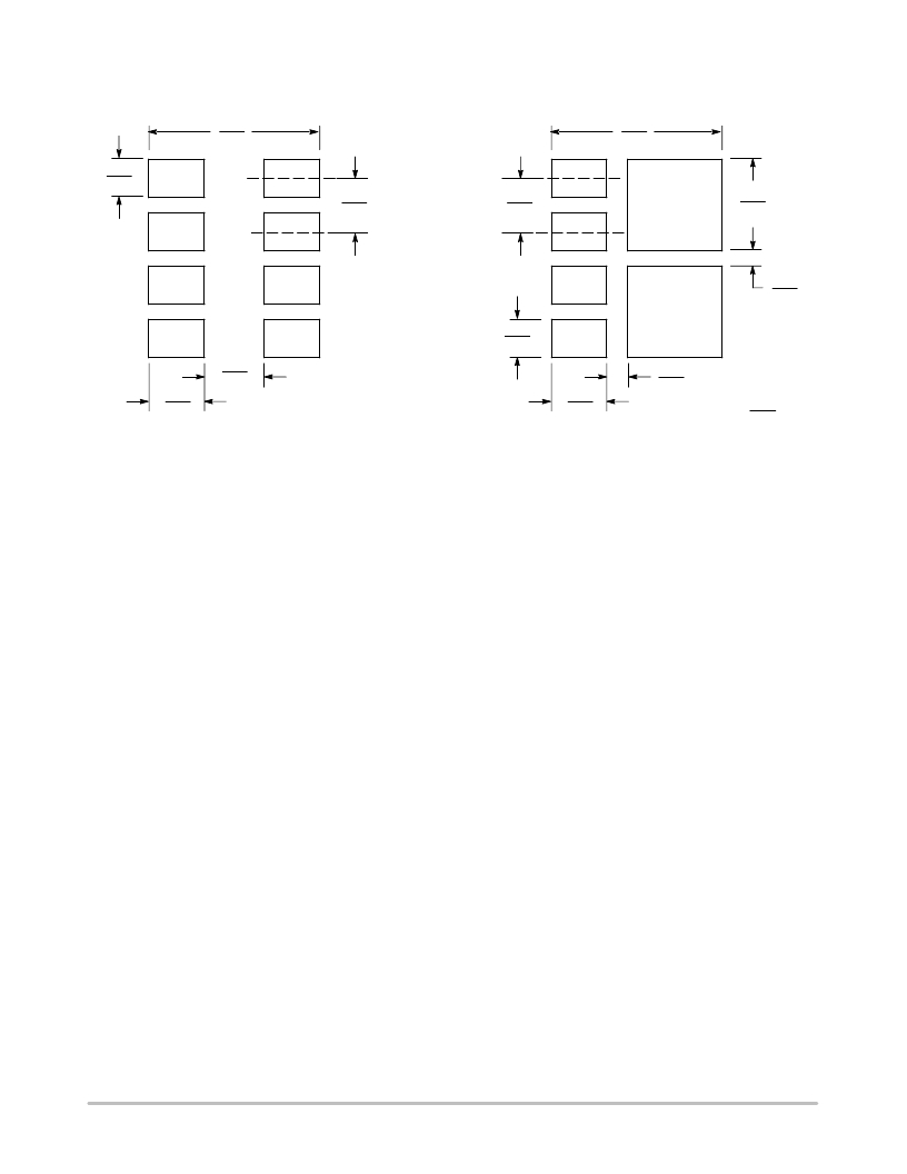
SOLDERING FOOTPRINT*
0 .45 7
2 .03 2
0.08
2.03 2
0.08
0.018
0 .63 5
0.025
0 .63 5
0.025
1 .09 2
0.043
0 .17 8
0.007
0 .45 7
0.018
0.66
0.026
0.711
0.028
0.66
0.026
0.25 4
0.010
SCALE 20:1
mm
inches
Figure 12. Basic
Figure 13. Style 2
*For additional information on our Pb?Free strategy and soldering
details, please download the ON Semiconductor Soldering and
Mounting Techniques Reference Manual, SOLDERRM/D.
BASIC PAD PATTERNS
The basic pad layout with dimensions is shown in
Figure 12. This is sufficient for low power dissipation
MOSFET applications, but power semiconductor
performance requires a greater copper pad area,
particularly for the drain leads.
The minimum recommended pad pattern shown in
Figure 13 improves the thermal area of the drain
confines of the basic footprint. The drain copper area is
0.0019 sq. in. (or 1.22 sq. mm). This will assist the power
dissipation path away from the device (through the copper
leadframe) and into the board and exterior chassis (if
applicable) for the single device. The addition of a further
copper area and/or the addition of vias to other board layers
will enhance the performance still further.
connections (pins 5, 6, 7, 8) while remaining within the
http://onsemi.com
5
发布紧急采购,3分钟左右您将得到回复。
相关PDF资料
NTHD5904NT1G
MOSFET N-CHAN 3.3A 20V CHIPFET
NTHS2101PT1
MOSFET P-CH 8V 5.4A CHIPFET
NTHS4101PT1G
MOSFET P-CH 20V 4.8A CHIPFET
NTHS4166NT1G
MOSFET N-CH 30V 4.9A CHIPFET
NTHS4501NT1G
MOSFET N-CH 30V 4.9A CHIPFET
NTHS5404T1G
MOSFET N-CH 20V 5.2A CHIPFET
NTHS5441T1G
MOSFET PWR P-CH 3.9A 20V CHIPFET
NTHS5443T1
MOSFET P-CH 20V 3.6A CHIPFET
相关代理商/技术参数
NTHD5904N
制造商:ONSEMI 制造商全称:ON Semiconductor 功能描述:Power MOSFET 20 V, 4.5 A, Dual N−Channel, ChipFET
NTHD5904N_05
制造商:ONSEMI 制造商全称:ON Semiconductor 功能描述:Power MOSFET 20 V, 4.5 A, Dual N−Channel, ChipFET
NTHD5904NT1
功能描述:MOSFET 20V 4.5A Dual RoHS:否 制造商:STMicroelectronics 晶体管极性:N-Channel 汲极/源极击穿电压:650 V 闸/源击穿电压:25 V 漏极连续电流:130 A 电阻汲极/源极 RDS(导通):0.014 Ohms 配置:Single 最大工作温度: 安装风格:Through Hole 封装 / 箱体:Max247 封装:Tube
NTHD5904NT1G
功能描述:MOSFET 20V 4.5A Dual N-Channel RoHS:否 制造商:STMicroelectronics 晶体管极性:N-Channel 汲极/源极击穿电压:650 V 闸/源击穿电压:25 V 漏极连续电流:130 A 电阻汲极/源极 RDS(导通):0.014 Ohms 配置:Single 最大工作温度: 安装风格:Through Hole 封装 / 箱体:Max247 封装:Tube
NTHD5904NT3
功能描述:MOSFET 20V 4.5A Dual RoHS:否 制造商:STMicroelectronics 晶体管极性:N-Channel 汲极/源极击穿电压:650 V 闸/源击穿电压:25 V 漏极连续电流:130 A 电阻汲极/源极 RDS(导通):0.014 Ohms 配置:Single 最大工作温度: 安装风格:Through Hole 封装 / 箱体:Max247 封装:Tube
NTHD5904NT3G
功能描述:MOSFET 20V 4.5A Dual N-Channel RoHS:否 制造商:STMicroelectronics 晶体管极性:N-Channel 汲极/源极击穿电压:650 V 闸/源击穿电压:25 V 漏极连续电流:130 A 电阻汲极/源极 RDS(导通):0.014 Ohms 配置:Single 最大工作温度: 安装风格:Through Hole 封装 / 箱体:Max247 封装:Tube
NTHD5904T1
功能描述:MOSFET 2N-CH 20V 3.1A CHIPFET RoHS:否 类别:分离式半导体产品 >> FET - 阵列 系列:- 产品目录绘图:8-SOIC Mosfet Package 标准包装:1 系列:- FET 型:2 个 N 沟道(双) FET 特点:逻辑电平门 漏极至源极电压(Vdss):60V 电流 - 连续漏极(Id) @ 25° C:3A 开态Rds(最大)@ Id, Vgs @ 25° C:75 毫欧 @ 4.6A,10V Id 时的 Vgs(th)(最大):3V @ 250µA 闸电荷(Qg) @ Vgs:20nC @ 10V 输入电容 (Ciss) @ Vds:- 功率 - 最大:1.4W 安装类型:表面贴装 封装/外壳:PowerPAK? SO-8 供应商设备封装:PowerPAK? SO-8 包装:Digi-Reel® 产品目录页面:1664 (CN2011-ZH PDF) 其它名称:SI7948DP-T1-GE3DKR
NTHD5904T1/D
制造商:未知厂家 制造商全称:未知厂家 功能描述:Power MOSFET Dual N-Channel
